- 您现在的位置:买卖IC网 > Sheet目录329 > IDT70V5388S166BGI (IDT, Integrated Device Technology Inc)IC SRAM 1.125MBIT 166MHZ 272BGA
IDT70V5388/78
3.3V 64/32K x 18 Synchronous FourPort? Static RAM
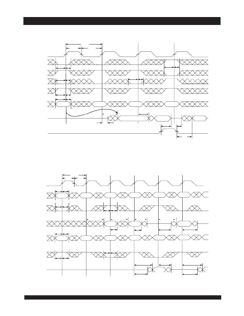
Switching Waveforms
Timing Waveform of Read Cycle (2)
t CYC2
Industrial and Commercial Temperature Ranges
CLK
CE 0
t CH2
t CL2
t SC
t HC
t SC
t HC
(3)
CE 1
LB , UB
R/ W
t SB
t SW
t SA
t HB
t HW
t HA
t SB
(5)
t HB
ADDRESS
(4)
An
An + 1
An + 2
An + 3
(1 Latency)
t CD2
t DC
DATA OUT
t CKLZ
(1)
Qn
Qn + 1
t OHZ
t OLZ
Qn + 2
(5)
NOTES:
OE
(1)
t OE
,
1. OE is asynchronously controlled; all other inputs are synchronous to the rising clock edge.
2. CNTLD = V IL , CNTINC and CNTRST = V IH .
5649 drw 08
3. The output is disabled (High-Impedance state) by CE 0 = V IH , CE 1 = V IL , LB , UB = V IH following the next rising edge of the clock. Refer to Truth Table I.
4. Addresses do not have to be accessed sequentially since CNTLD = V IL constantly loads the address on the rising edge of the CLK; numbers
are for reference use only.
5. If LB , UB was HIGH, then the appropriate Byte of DATA OUT for Qn + 2 would be disabled (High-Impedance state).
Timing Waveform of a Multi-Device Read (1,2)
t CYC2
CLK
t CH2
t CL2
t SA
t HA
ADDRESS (B1)
A 0
A 1
A 2
A 3
A 4
A 5
A 6
t SC
t HC
CE 0(B1)
t SC
t HC
DATA OUT(B1)
t CD2
Q 0
t CD2
Q 1
t CKHZ
t CD2
Q 3
t SA
t HA
t DC
t DC
t CKLZ
t CKHZ
ADDRESS (B2)
A 0
A 1
A 2
A 3
A 4
A 5
A 6
t SC
t HC
CE 0(B2)
t SC
t HC
t CD2
t CKHZ
t CD2
DATA OUT(B2)
NOTES:
t CKLZ
Q 2
t CKLZ
Q 4
5649 drw 09
,
1. B1 Represents Device #1; B2 Represents Device #2. Each Device consists of one IDT70V5388/78 for this waveform,
and are setup for depth expansion in this example. ADDRESS (B1) = ADDRESS (B2) in this situation.
2. LB , UB , OE , and CNTLD = V IL ; CE 1(B1) , CE 1(B2) , R/ W , CNTINC , and CNTRST = V IH .
14
发布紧急采购,3分钟左右您将得到回复。
相关PDF资料
IDT70V631S10PRFG
IC SRAM 4MBIT 10NS 128TQFP
IDT70V639S12PRFI
IC SRAM 2.25MBIT 12NS 128TQFP
IDT70V659S12DRI
IC SRAM 4MBIT 12NS 208QFP
IDT70V7319S166BCI
IC SRAM 4MBIT 166MHZ 256BGA
IDT70V7339S166BCI
IC SRAM 9MBIT 166MHZ 256BGA
IDT70V7519S166DRI
IC SRAM 9MBIT 166MHZ 208QFP
IDT70V7599S133DRI
IC SRAM 4MBIT 133MHZ 208QFP
IDT70V9089L6PF
IC SRAM 512KBIT 6NS 100TQFP
相关代理商/技术参数
IDT70V5388S166BGI8
功能描述:IC SRAM 1.125MBIT 166MHZ 272BGA RoHS:否 类别:集成电路 (IC) >> 存储器 系列:- 标准包装:3,000 系列:- 格式 - 存储器:EEPROMs - 串行 存储器类型:EEPROM 存储容量:8K (1K x 8) 速度:400kHz 接口:I²C,2 线串口 电源电压:1.7 V ~ 5.5 V 工作温度:-40°C ~ 85°C 封装/外壳:8-SOIC(0.154",3.90mm 宽) 供应商设备封装:8-SOIC 包装:带卷 (TR)
IDT70V5388S200BC
功能描述:IC SRAM 1.125MBIT 200MHZ 256BGA RoHS:否 类别:集成电路 (IC) >> 存储器 系列:- 标准包装:3,000 系列:- 格式 - 存储器:EEPROMs - 串行 存储器类型:EEPROM 存储容量:8K (1K x 8) 速度:400kHz 接口:I²C,2 线串口 电源电压:1.7 V ~ 5.5 V 工作温度:-40°C ~ 85°C 封装/外壳:8-SOIC(0.154",3.90mm 宽) 供应商设备封装:8-SOIC 包装:带卷 (TR)
IDT70V5388S200BC8
功能描述:IC SRAM 1.125MBIT 200MHZ 256BGA RoHS:否 类别:集成电路 (IC) >> 存储器 系列:- 标准包装:3,000 系列:- 格式 - 存储器:EEPROMs - 串行 存储器类型:EEPROM 存储容量:8K (1K x 8) 速度:400kHz 接口:I²C,2 线串口 电源电压:1.7 V ~ 5.5 V 工作温度:-40°C ~ 85°C 封装/外壳:8-SOIC(0.154",3.90mm 宽) 供应商设备封装:8-SOIC 包装:带卷 (TR)
IDT70V5388S200BCG
功能描述:IC SRAM 1.125MBIT 200MHZ 256BGA RoHS:是 类别:集成电路 (IC) >> 存储器 系列:- 标准包装:3,000 系列:- 格式 - 存储器:EEPROMs - 串行 存储器类型:EEPROM 存储容量:8K (1K x 8) 速度:400kHz 接口:I²C,2 线串口 电源电压:1.7 V ~ 5.5 V 工作温度:-40°C ~ 85°C 封装/外壳:8-SOIC(0.154",3.90mm 宽) 供应商设备封装:8-SOIC 包装:带卷 (TR)
IDT70V5388S200BG
功能描述:IC SRAM 1.125MBIT 200MHZ 272BGA RoHS:否 类别:集成电路 (IC) >> 存储器 系列:- 标准包装:3,000 系列:- 格式 - 存储器:EEPROMs - 串行 存储器类型:EEPROM 存储容量:8K (1K x 8) 速度:400kHz 接口:I²C,2 线串口 电源电压:1.7 V ~ 5.5 V 工作温度:-40°C ~ 85°C 封装/外壳:8-SOIC(0.154",3.90mm 宽) 供应商设备封装:8-SOIC 包装:带卷 (TR)
IDT70V5388S200BG8
功能描述:IC SRAM 1.125MBIT 200MHZ 272BGA RoHS:否 类别:集成电路 (IC) >> 存储器 系列:- 标准包装:3,000 系列:- 格式 - 存储器:EEPROMs - 串行 存储器类型:EEPROM 存储容量:8K (1K x 8) 速度:400kHz 接口:I²C,2 线串口 电源电压:1.7 V ~ 5.5 V 工作温度:-40°C ~ 85°C 封装/外壳:8-SOIC(0.154",3.90mm 宽) 供应商设备封装:8-SOIC 包装:带卷 (TR)
IDT70V631S10BC
功能描述:IC SRAM 4MBIT 10NS 256BGA RoHS:否 类别:集成电路 (IC) >> 存储器 系列:- 标准包装:2,500 系列:- 格式 - 存储器:EEPROMs - 串行 存储器类型:EEPROM 存储容量:1K (128 x 8) 速度:100kHz 接口:UNI/O?(单线) 电源电压:1.8 V ~ 5.5 V 工作温度:-40°C ~ 85°C 封装/外壳:8-TSSOP,8-MSOP(0.118",3.00mm 宽) 供应商设备封装:8-MSOP 包装:带卷 (TR)
IDT70V631S10BC8
功能描述:IC SRAM 4MBIT 10NS 256BGA RoHS:否 类别:集成电路 (IC) >> 存储器 系列:- 标准包装:3,000 系列:- 格式 - 存储器:EEPROMs - 串行 存储器类型:EEPROM 存储容量:8K (1K x 8) 速度:400kHz 接口:I²C,2 线串口 电源电压:1.7 V ~ 5.5 V 工作温度:-40°C ~ 85°C 封装/外壳:8-SOIC(0.154",3.90mm 宽) 供应商设备封装:8-SOIC 包装:带卷 (TR)
